Common Circuit Board Manufacturing Techniques Explained
by Suntop
2025-12-04
Circuit boards are the backbone of modern electronics. They connect and support electronic components, making devices function. Understanding how they are made is crucial for anyone in the electronics field.
The manufacturing of circuit boards involves several techniques. Each technique plays a vital role in the final product’s performance. From design to assembly, every step is important.
Printed Circuit Boards (PCBs) are the most common type. They are used in everything from smartphones to industrial machines. Their design and manufacturing require precision and expertise.
Materials like fiberglass and epoxy are used in PCB production. These materials ensure durability and reliability. The choice of materials can affect the board’s performance and cost.
Two main methods for mounting components are Surface Mount Technology (SMT) and Through-Hole Technology (THT). SMT allows for compact designs, while THT offers strong mechanical bonds.
Quality control is essential in PCB manufacturing. It ensures that the boards function correctly and reliably. Without it, devices could fail.
Advances in PCB technology continue to drive innovation. New materials and techniques are constantly being developed. This keeps the electronics industry moving forward.
What Is a Circuit Board? Understanding the Basics
A circuit board is a crucial component in electronics, serving as the foundation for circuitry. It supports and connects electronic components electrically and mechanically. But what exactly is it made of?
Circuit boards, commonly known as Printed Circuit Boards (PCBs), are integral in all types of electronics. Their primary role is to support and connect various electronic components. Without them, our devices wouldn’t function.
PCBs are typically composed of non-conductive substrates, like fiberglass. Copper layers are etched onto this substrate to create the necessary circuit pathways. This conductive material forms the network needed for electricity to flow.
There are several main elements of a circuit board, including:
- Substrate: Provides mechanical support.
- Copper layer: Conducts electricity.
- Solder mask: Protects the copper.
- Silkscreen: Offers labeling for assembly.
Creating a circuit board involves precision and attention to detail. Manufacturers use meticulous techniques to ensure quality and performance. This involves translating a schematic design onto a physical board.
The terms we often hear associated with PCBs might include “PC board” or “electronic board”. These terms all refer to the same vital piece of technology. Understanding these concepts is essential for electronics enthusiasts and professionals alike.
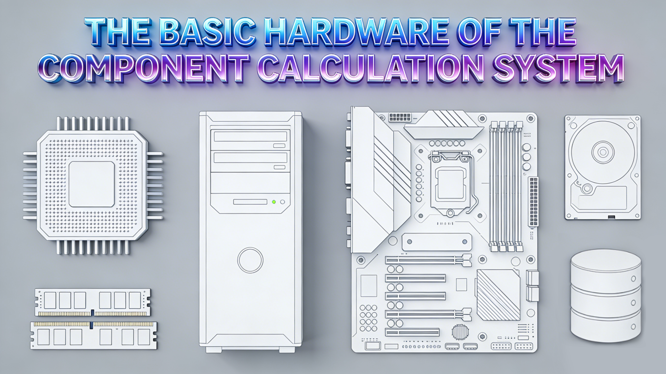
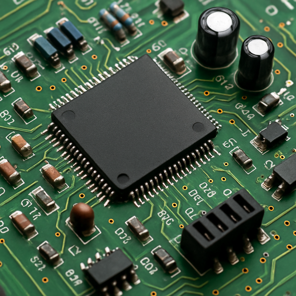
Key Components of a PCB: What Makes Up a Circuit Board?
Printed Circuit Boards (PCBs) are complex yet fascinating, comprising several essential components. Each piece serves a unique purpose in the overall function of the board.
At the heart of a PCB is the substrate, usually made from fiberglass. This layer provides the board with the necessary rigidity and insulation. It’s the backbone on which all other components rest.
Copper traces are another critical part. They are thin strips of copper that create pathways for electrical currents. Without these, connecting electronic components would be impossible.
The solder mask is what gives a PCB its characteristic green color. It insulates the copper traces, preventing unintentional contact or short-circuits. This layer keeps everything on the board running smoothly.
Additional elements of a PCB include:
- Silkscreen: Labels components for easy identification.
- Resistors: Control current flow.
- Capacitors: Store electrical energy.
- Diodes: Allow current to pass in one direction.
- Transistors and ICs (Integrated Circuits): Form the logic of many devices.
These components collectively make up a PCB, enabling it to power and control electronic devices effectively.
Types of Circuit Boards: Single-Sided, Double-Sided, and Multilayer
Circuit boards come in various types, each suited for different applications. Understanding these types helps in selecting the right board for a project.
Single-sided PCBs are the simplest form. They have components on one side and a conductive path on the other. These are common in low-cost and simple electronics.
Double-sided PCBs allow components and conductive paths on both sides. This doubles the circuit area without increasing the board size. They are perfect for moderate-complexity devices.
Multilayer PCBs are more advanced, having multiple layers of substrate and copper traces. These are used in complex applications like computers or servers. They provide greater circuit density and flexibility.
The choice of a PCB type depends on several factors:
- Device complexity
- Required component density
- Available space
- Cost considerations
Each board type serves distinct purposes, offering different levels of complexity and functionality. Understanding these differences aids in efficient design and application.
For instance, while single-sided boards are cost-effective, multilayer boards allow more intricate circuits. This is crucial for devices requiring high performance and reliability.
Selecting the proper PCB type is pivotal for device efficiency and functionality. It’s essential for engineers and hobbyists alike.
Materials Used in PCB Manufacturing
The choice of materials in PCB manufacturing greatly influences performance and durability. Different materials cater to varying needs in electronic devices.
Fiberglass, often in the form of FR-4, is the most common substrate. It provides excellent mechanical strength and electrical insulation. This material is favored for its reliability and ability to withstand high temperatures.
Composite epoxy materials are also popular. They offer flexibility in design and are useful for complex boards. Their lightweight nature is an added advantage for portable devices.
Copper is essential for conducting paths. It’s used extensively due to its excellent conductivity. The thickness of the copper layer varies based on the board’s electrical requirements.
Additional materials used include:
- Aluminum, for heat dissipation in power applications
- Polyimide, for flexible circuits
- Glass-reinforced epoxy, for strength and moisture resistance
The selection of these materials is crucial, affecting the PCB’s functionality and cost. Choosing wisely can lead to significant performance improvements in electronic devices.
The PCB Design Process: From Schematic to Layout
Designing a PCB is a meticulous process, beginning with a detailed schematic. This blueprint forms the basis for the entire design.
Engineers use specialized software to create the schematic. This tool allows them to visualize connections between circuit components. Proper labeling and component placement are crucial at this stage.
After the schematic, the next step is the layout. This involves arranging components on the board itself. Space management is vital to prevent overcrowding and ensure functionality.
During the layout phase, engineers consider several factors:
- Signal integrity
- Thermal management
- Power distribution
- Component placement
- Via locations
Routing paths between components is also a key task. This requires precision to minimize interference and enhance performance. Tools like auto-routers can automate some of this work, increasing efficiency.
Once the layout is finalized, it undergoes a verification process. This step checks for design rule compliance and potential errors. It ensures that the final PCB can be manufactured without issues.
The design process is crucial in PCB manufacturing. It provides a foundation, impacting both the device’s performance and reliability.
Step-by-Step PCB Manufacturing Process
Manufacturing a PCB involves multiple steps, each crucial to the final product.
The process begins with designing the circuit pattern. This pattern is then transferred onto a laminate board.
Next, the unwanted copper is removed through etching. This step leaves the desired circuit paths intact.
Drilling follows, where holes are created for component leads and vias. These holes enable connections between PCB layers.
Layers are then aligned and laminated, forming multi-layer boards when needed. This step requires precision to ensure layer accuracy.
After lamination, the board undergoes plating and finishing. This adds a conductive layer, enhancing durability.
A solder mask is applied next, protecting circuits from damage. The silkscreen layer follows, helping identify components and connections.
Finally, profiling shapes the board, making it ready for assembly. Routing refines edges, while cutting defines the board’s structure.
Throughout these steps, quality control checks ensure reliability. Each phase is critical to creating a functional PCB.
Step 1: Imaging and Printing the Circuit Pattern
Imaging is the first detailed step in PCB production. It involves transferring the circuit design onto the board.
The PCB design is printed on a transparent film. This film acts like a stencil for the board.
A photoresist coating is then applied to the copper layer of the board. The transparent film is placed over it.
The board is exposed to ultraviolet light, hardening areas not covered by the design. This leaves a precise circuit pattern on the board.
Step 2: Etching and Removing Unwanted Copper
Etching is where unnecessary copper is removed. This process defines the pathways on the PCB.
After imaging, the board is submerged in an acidic solution. The acid eats away the unexposed copper areas.
Only the protected circuit paths remain intact. The result is a clean and precise circuit pattern ready for further processing.
Step 3: Drilling and Creating Vias
Drilling creates holes for component pins and vias. This step connects different circuit layers.
Precision drills puncture the board at specified locations. These holes accommodate electronic components.
Vias are also drilled to facilitate inter-layer connectivity. Special machines ensure accuracy and uniformity in hole sizes.
Step 4: Layer Alignment and Lamination
Aligning and laminating layers is crucial for multi-layer PCBs. It ensures each layer is correctly positioned.
Boards are stacked in precise order. Holes and alignment marks guide the stacking process.
Lamination follows, bonding the layers with heat and pressure. The result is a single, solid board ready for plating.
Step 5: Plating and Surface Finishing
Plating is essential to add a conductive layer. It improves connections and protects circuit paths.
The board undergoes electroless plating. It involves depositing a thin metal layer over exposed copper.
Surface finishing options include:
- Gold plating
- Silver immersion
- Organic solderability preservative
- These finishes enhance durability and performance.
Step 6: Solder Mask and Silkscreen Application
A solder mask is applied to shield circuits from environmental damage. It also prevents solder bridges.
The mask is a colored polymer film laid over the board. It leaves exposed areas where components will be soldered.
Afterward, the silkscreen layer is added. This provides labels and markings, crucial for assembly and troubleshooting.
Step 7: Profiling, Routing, and Final Shaping
Profiling shapes the board edges. Accurate dimensions are essential for fitting into devices.
Routing cuts the board from the larger panel. This step defines the board’s final size and shape.
Profiling ensures smooth edges, preventing damage during handling or assembly. The board is now ready for component mounting
Component Mounting Techniques: SMT vs. THT
Mounting electronic components is a critical part of PCB assembly. Two primary techniques are used: Surface Mount Technology (SMT) and Through-Hole Technology (THT).
SMT involves mounting components directly onto the surface of the PCB. This method allows for smaller components and more compact designs.
In SMT, components are placed on pads without needing drilled holes. This technique is ideal for high-density applications.
THT, on the other hand, uses leads inserted into drilled holes. These are then soldered to pads on the opposite side of the board.
THT provides robust mechanical bonding, making it suitable for components that endure physical stress. It’s also preferred when reliability under harsh conditions is required.
THT, on the other hand, uses leads inserted into drilled holes. These are then soldered to pads on the opposite side of the board.
- THT provides robust mechanical bonding, making it suitable for components that endure physical stress. It’s also preferred when reliability under harsh conditions is required.
Choosing between SMT and THT depends on application needs and space constraints. Both play pivotal roles in modern electronics manufacturing.
Quality Control and Testing in PCB Manufacturing
Quality control is vital in PCB manufacturing. It ensures reliability and performance in the final product.
Several steps are taken to maintain high standards. These include visual inspections and automated testing processes.
Functional testing is essential. It checks if the PCB performs its intended task without errors.
Common Quality Control Methods:
- Visual Inspection: Detects obvious flaws like misalignments.
- Automated Optical Inspection (AOI): Uses cameras to scan boards for anomalies.
- X-ray Inspection: Reveals internal problems not visible to the eye.
- Function Testing: Evaluates the board’s performance under real-world conditions.
Testing helps identify defects and correct them early. This helps avoid costly returns and device failures later.
By ensuring thorough testing, manufacturers uphold their reputation for quality. This builds trust with customers and supports long-term success in the industry.
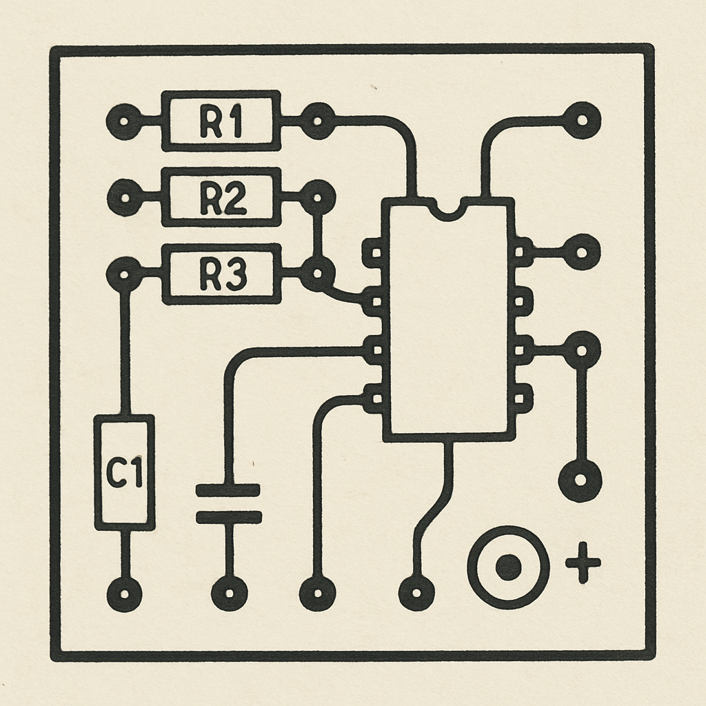
How to Read a PCB: Understanding Circuit Board Layouts
Reading a PCB requires understanding its layout. It begins with recognizing the components and their arrangement.
Each component on a PCB is labeled. This is usually done with silkscreen markings, making identification easier.
Key elements to identify include:
- Traces: These are the paths that connect different components.
- Pads: Areas where component leads are soldered.
- Vias: Holes that allow connection between board layers.
To read a PCB effectively, follow the traces. Observe how they connect components and form circuits.
Familiarity with symbols and abbreviations enhances comprehension. This skill proves invaluable for troubleshooting and repairs.
A systematic approach aids in quick identification. This helps in assessing any potential issues with the PCB’s design or function.
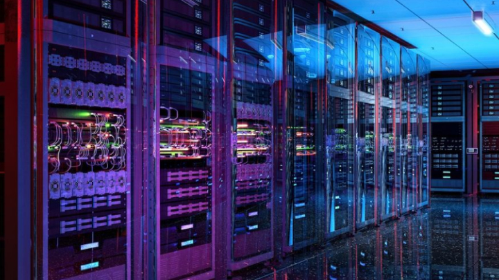
Applications of Circuit Boards: Where Are PCBs Used?
Printed Circuit Boards (PCBs) play a vital role in various devices. They’re essential in numerous applications, from everyday gadgets to complex machinery.
PCBs facilitate compact and efficient designs. This makes them crucial in consumer electronics, industrial controls, and beyond.
Common applications include:
- Computers and smartphones
- Automotive electronics
- Medical devices
- Telecommunication equipment
- Aerospace instrumentation
Their versatility allows for integration in diverse fields. This adaptability ensures their presence in cutting-edge technology.
As innovation drives electronics, PCBs continue to evolve. Their applications broaden, meeting the demands of modern devices.
Advances and Trends in PCB Manufacturing
The world of PCB manufacturing is dynamic and ever-changing. Innovations are continually reshaping how PCBs are produced and utilized.
Flexibility is a significant trend. Flexible PCBs are increasingly popular, allowing for bending and twisting in design.
New materials are also influencing PCB manufacturing. These materials enhance performance, reduce weight, and improve thermal management.
Key trends in the industry include:
- Integration of advanced materials
- Rise of flexible and wearable PCBs
- Increase in miniaturization
- Use of environmentally friendly practices
Automation is another critical advancement. It’s streamlining production, ensuring higher precision, and lowering costs.
The future of PCB manufacturing looks promising. These trends support the development of more robust, efficient, and versatile circuit boards.
Environmental Considerations in PCB Production
PCB production has environmental impacts that cannot be ignored. Manufacturers are adopting eco-friendly practices to minimize these effects.
These practices involve:
- Reducing waste
- Using sustainable materials
- Minimizing toxic substances
- Implementing recycling processes
Efforts focus on reducing the carbon footprint. This is achieved through energy-efficient processes and by selecting biodegradable materials.
Sustainable practices in PCB production are not just trends. They are essential steps toward a healthier planet. Manufacturers strive to balance innovation with environmental responsibility.
Conclusion: The Future of Circuit Board Manufacturing
The future of circuit board manufacturing shines bright. With rapid advancements, new technologies continue to emerge.
Flexible PCBs are gaining popularity. They offer versatile applications in wearable and portable gadgets.
Incorporating sustainable practices will be paramount. This ensures eco-friendliness alongside cutting-edge innovation. As technology evolves, PCBs will remain the backbone of electronic evolution.
SUNTOP
Founded in 2000, Suntop is one of the leading global distributors of electronic components, dedica ted to providing comprehensive procurement and supply chain services to the global electronics manufacturing industry. Our services include distribution, spot trading, PPV cost-saving projects, and inventory management. We not only offer high-quality products but also strive to assist our clients in achieving optimal solutions with minimal time and cost.
Suntop is a popular choice for those seeking electron devices and circuits due to their competitive pricing and reliable service. They cater to both small-scale hobbyists and large-scale manufacturers, ensuring that every customer finds what they need.

SHARE: